Samsung LEDs a circle integrated with 4 parts: thermal management, structural analysis, materials, optics, while LED modules are located in the center of the circle, with the laboratory background in black and white (key visual, desktop)
A Broad Understanding of LED Technology

Recently, LED lighting is gaining in popularity and customers are becoming more demanding about product performance. LED component vendors are also under pressure from their corporate customers to come up with solutions that go beyond their traditional business portfolio.

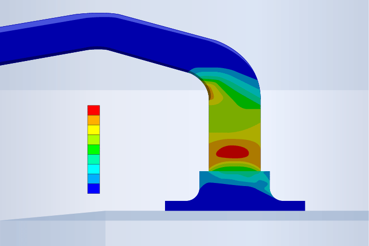
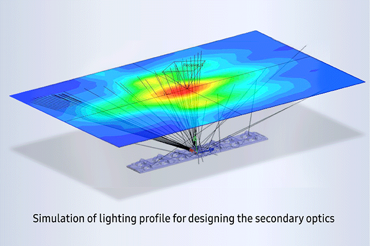
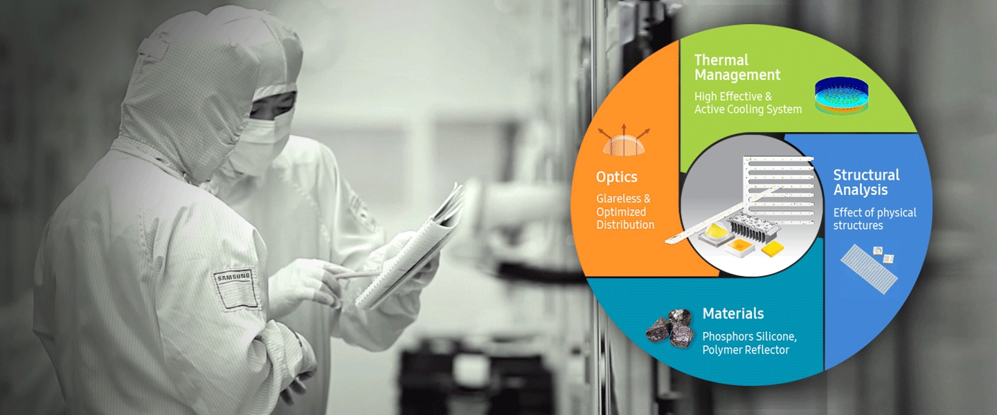
Samsung Electronics has been in the LED business for more than 10 years, covering a range of applications in indoor and outdoor lighting, displays, and the automotive market. It is an industry leader in terms of both product performance and technological prowess in fundamental technologies related to materials, optics, heating and structural analysis, all of which contribute to our ability to deliver what customers want.

Samsung LEDs a simplified cross-section of a LED package with a phrase: high efficay that comes with high reliability
Materials - High Transparency Encap./Film Silicone

Samsung has continuously developed and applied high refractive index silicon materials to improve LED efficiency through higher light extraction. High-refraction silicon keeps optical loss due to total reflection at the chip / silicon interface to a minimum, resulting in higher light efficiency. Reliability, however, is another matter, and something on which Samsung is focused on improving.

Material - High Reliability Solder/Bonder

Applying Samsung’s exclusive flip chip technology to a package is dependent on whether we can produce an excellent fatigue- and stress-resistant solder material. Samsung uses solder materials that are eco-friendly and reliable, Pb-free and Sn-based. We have also developed a range of bonding materials that can improve product reliability, including anti-shrinkage bonding for epi-chips and high-conductivity Ag epoxy adhesives.

Samsung LEDs two LED packages: one using white silicone; and the other containing a reflector
Material - Superior White Reflector

Samsung is also working on improving the reflectance of PCT, EMC and other molding materials for PLCC (plastic leaded chip carrier) type LED products. More recently, our focus is on developing high-strength white silicon mainly for the new chip scale package platform.

Samsung LEDs a heat distribution image of the ceramic LED package
Thermal Analysis - Reliable & Efficient LED

The performance and longevity of any LED device or module essentially depend on how well the heat generated by the light source is controlled. Heat generated from junctions in the device compromises the materials making up the LED package and module, undermining their performance and consequently reducing their life span. Heat from phosphors or junctions in the device is dissipated into the atmosphere through encapsulant and the lens or through the substrate.

Through more accurate predictions of heat flow inside LED devices, Samsung is working to improve structural design of devices and optimize materials , towards the ultimate goal of boosting LED device performance and life expectancy.

Samsung LEDs a heat distribution image of the LED module
Thermal Analysis - Efficient Module Assembly

An LED module consists of multiple LED devices, PCB and a variety of other parts, so the heat generated by an entire module depends on heat dissipation from the heat sink and the amount of heat generated by the sum of its parts. PCB module and heat sink materials and structural design, and placement of the various parts can also improve module performance and life expectancy. Samsung uses its practical experience with heat dissipation technology to give you light source solutions that will meet your demands.

Samsung LEDs a structural stress distribution image of the LED device
Structural Stress Analysis - Improving Process Optimization

When in use, an LED device is mounted on a set and exposed to repeated cycles of high and low temperatures. This persistent stress causes thermal deformation of the encapsulant, lead frame, or mold, which results in stress accumulation on the wire / solder and lighting failure if that wire breaks.

Samsung has been seeking to optimize the material and shape of its wire / solder and package board components to delay the fatigue breakdown point and thereby improve overall product quality and life expectancy. This structural analysis technology is applied to package wire bonding as well as to the more general package and module structure design. It is also optimized for a range of other applications such as TVs, lighting and automotive products.

Samsung LEDs simulation of lighting profile for designing the secondary optics
Optical Solution

The light emitted from LED lighting is versatile as is, but not enough to meet the full range of customer needs: a secondary optical system is essential. Samsung uses its secondary optical design technology for LED light sources to develop products tailored to your specific applications.

Optic design is playing an increasingly important role in LED modules for TV, as more and more TV modules have adopted a secondary optical system to realize uniformity of screen display while maintaining the total number of LEDs at an optimal level. Samsung provides the optic design technology for any structure required, whether top-emitting or side-emitting. When it comes to modules for lighting, Samsung offers reflective and refractive optical systems that are flexible enough to meet diverse lighting needs in different countries or to match regulatory regimes. Our high-efficiency optical system enables maximum utility of LED light by minimizing loss. Automotive LED modules require extreme reliability, and different automakers seek different optical and fixture specifications. Samsung can offer customized optic solutions for automotive customers, including optic system structures that best suit their unique vehicle fixtures.

Samsung provides solutions that are free from any liabilities related to intellectual property, as they utilize patents exclusive to Samsung, facilitating production and sale of dependable products by its customers.

Samsung LEDs monte-carlo simulation of a complex optical stracture: accurate and sophisticated parametric modeling enables a faster development cycle
Optical Solution - Chips/PKG/Phosphor Modeling and Simulation

Samsung is capable of optical modeling simulations using the ray-tracing method, and can predict the optical characteristics of LED light source products consisting of LED chip devices, package and phosphor. In other words, we can simulate how a change in structure, shape, fabrication method, materials or physical properties of chips, packages, phosphors or encapsulations may affect light characteristics.

Our simulated analysis covers not only changes in the amount of light energy, such as luminous flux and luminous intensity, but also the quality of light, including beam angle, color temperature, and color variations by beam angle. Samsung also conducts optical mechanism analysis on these changes to find out why they occur.

These comprehensive technologies enable shorter time-to-market and reduced product development cost. Samsung's engineering capabilities allow it to design optimal packages by predicting the light characteristics of the package-embedded primary optical system and adjusting secondary system performance accordingly. These optical solutions form the foundation for the outstanding light quality of our devices and modules, and will undoubtedly add value to your products.

Contact Us Contact Us

We will help you find the right solutions for your business.

Sales Network Sales Network

Partner site for B2B collaboration