Samsung LEDs 8-inch wafers, and epitaxial growth of the GaN layer following the high pressure-grown buffer layer on the silicone substrate (key visual, desktop)
Si Technology

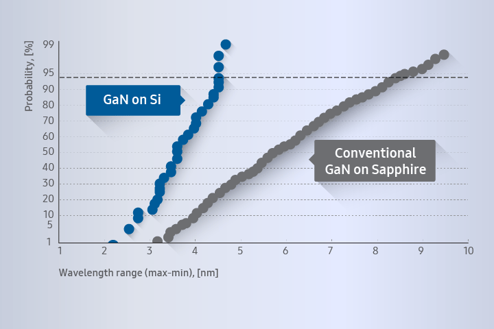
Samsung’s silicon-based LED technology has grown out of its semiconductor excellence, and is expected to change the paradigm of the LED industry, which has largely relied on sapphire substrate. As a substitute for sapphire, silicon will greatly decrease the cost of LED devices and still offer equivalent or even better light efficiency and uniformity.

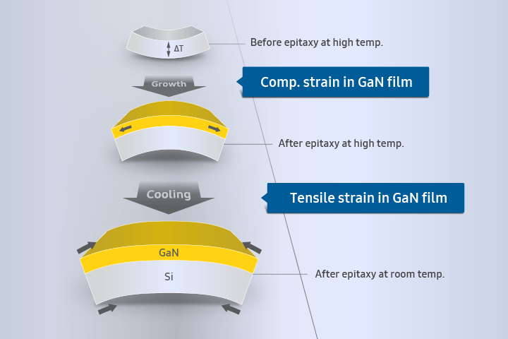
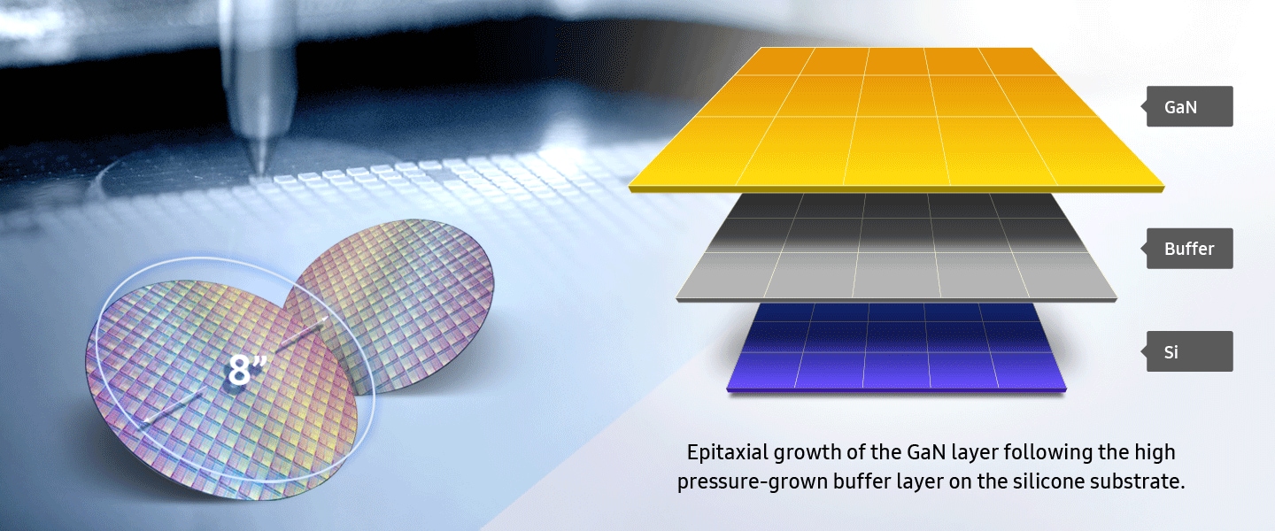
Samsung has introduced high-pressure growth technology to reduce dislocation caused by the lattice mismatch between the GaN and Si substrate, and improve crystalline quality of the LED structure. Chamber hardware has also been optimized to improve uniformity while maintaining high productivity.

Samsung LEDs improvements of Samsung's si technology: comp. strain in GaN film; tensile strain in GaN film
Si Technology - First in the Industry

Samsung LED's silicon technology is built on its semiconductor excellence. Any silicon-based LED production involves making large substrates, and most LED companies need to build a whole new infrastructure for this purpose only.

Samsung, on the other hand, is able to utilize its existing processing lines thanks to its well-established production of semiconductors, which gives it a significant edge: less initial overhead and shorter time-to-market. Samsung embarked on developing silicon-based LED in 2011, successfully commercializing it after two years. We are now improving performance and quality of Si-based products to widen the scope of applications.

Using Si substrates to grow LED structures is not as simple a technology as one might expect. While Si substrates are readily available in large diameters at lower cost than traditional sapphire substrates, the major technological challenge is to reduce stress and prevent defect caused by the lattice mismatch between GaN and Si.

Samsung LEDs a wavelength range-probability line graph that shows Samsung's GaN on Si leads to better uniformity compared to conventional GaN on Sapphire
Larger Wafer, Better Uniformity

Samsung has developed its own buffer layer technology to create a substrate environment optimized for growing light-emitting structures. A new growth method using high pressure has also been introduced to reduce defect and improve crystalline quality of the LED structure.

Samsung is undertaking a range of research activities to reach the highest level of uniformity for its Si-based LED structures in the world. Unlike sapphire substrates, Si substrates are commercially available in larger diameters, typically 8 inches or more. The key technological challenge is to attain high uniformity when growing the LED structures on the wafers. Samsung has optimized chamber hardware for better uniformity while maintaining high productivity, so that temperature and air flow within the chamber can be fine-tuned to improve dispersion.

Contact Us Contact Us

We will help you find the right solutions for your business.

Sales Network Sales Network

Partner site for B2B collaboration